Load & Start
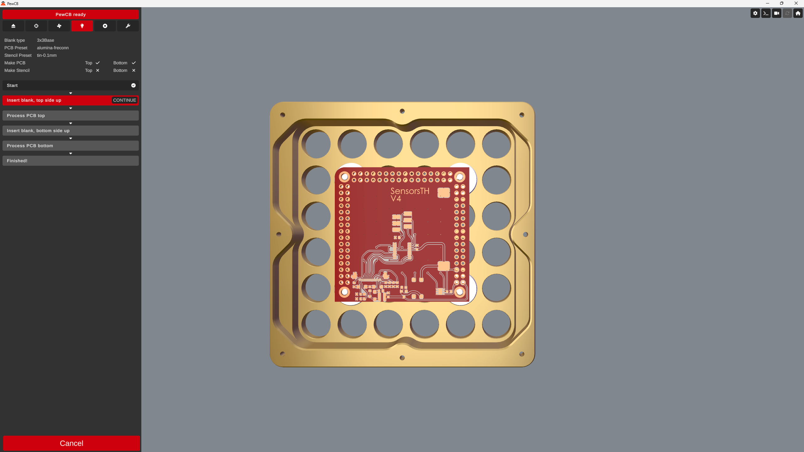
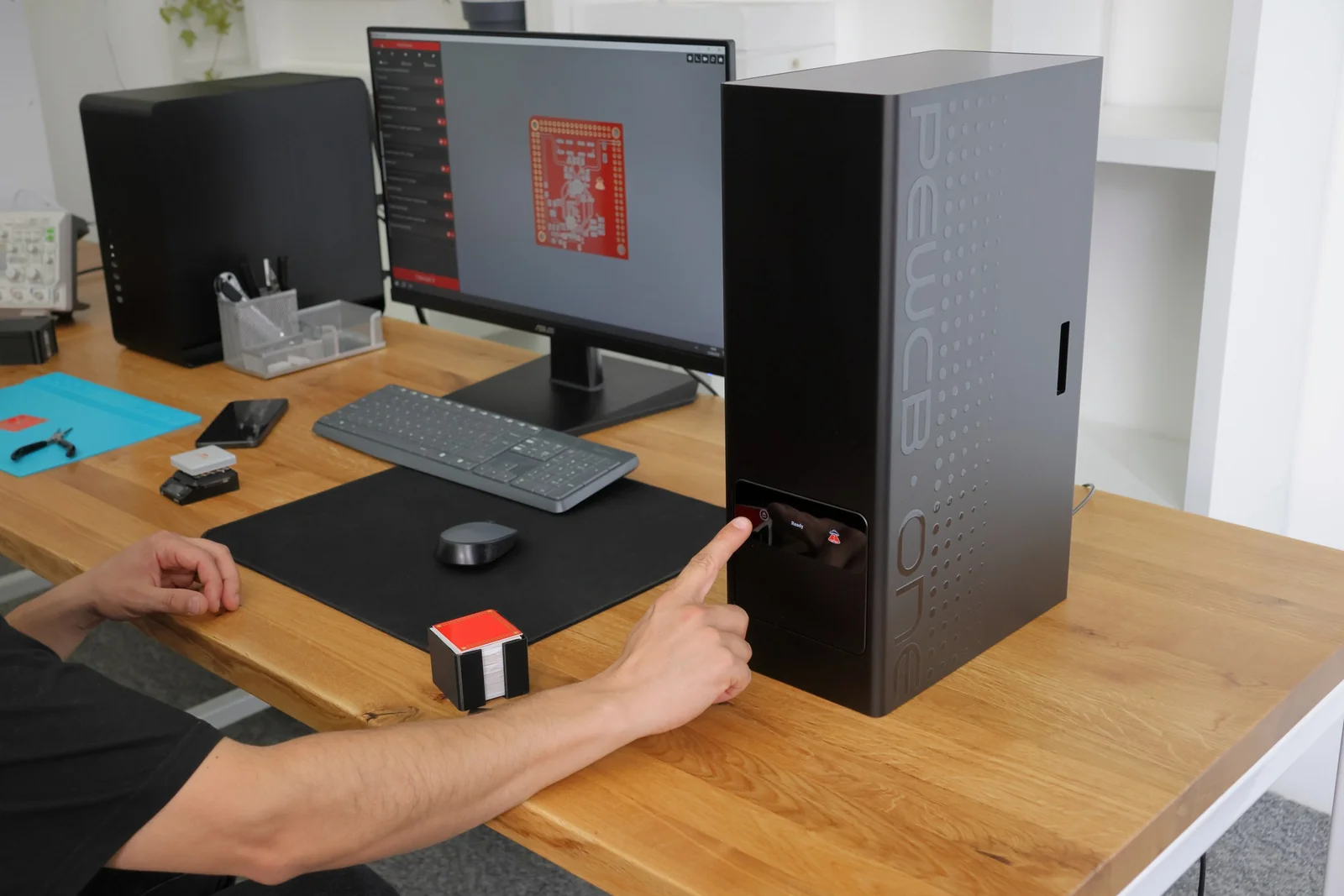
Open your Gerbers in the PewCB app, load a blank into the tray, and press Start.
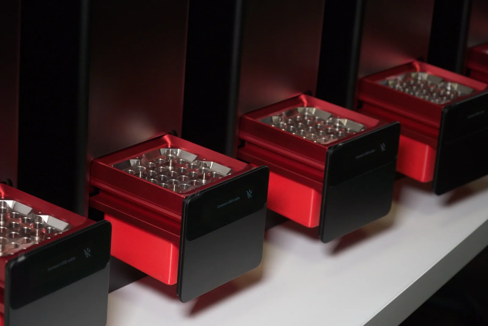
Desktop PCB prototyping machine
PewCB brings rapid circuit board prototyping directly to your desk. Eliminate fabrication lead times to test, fix, and build the next device revision the same day.
One continuous desktop process
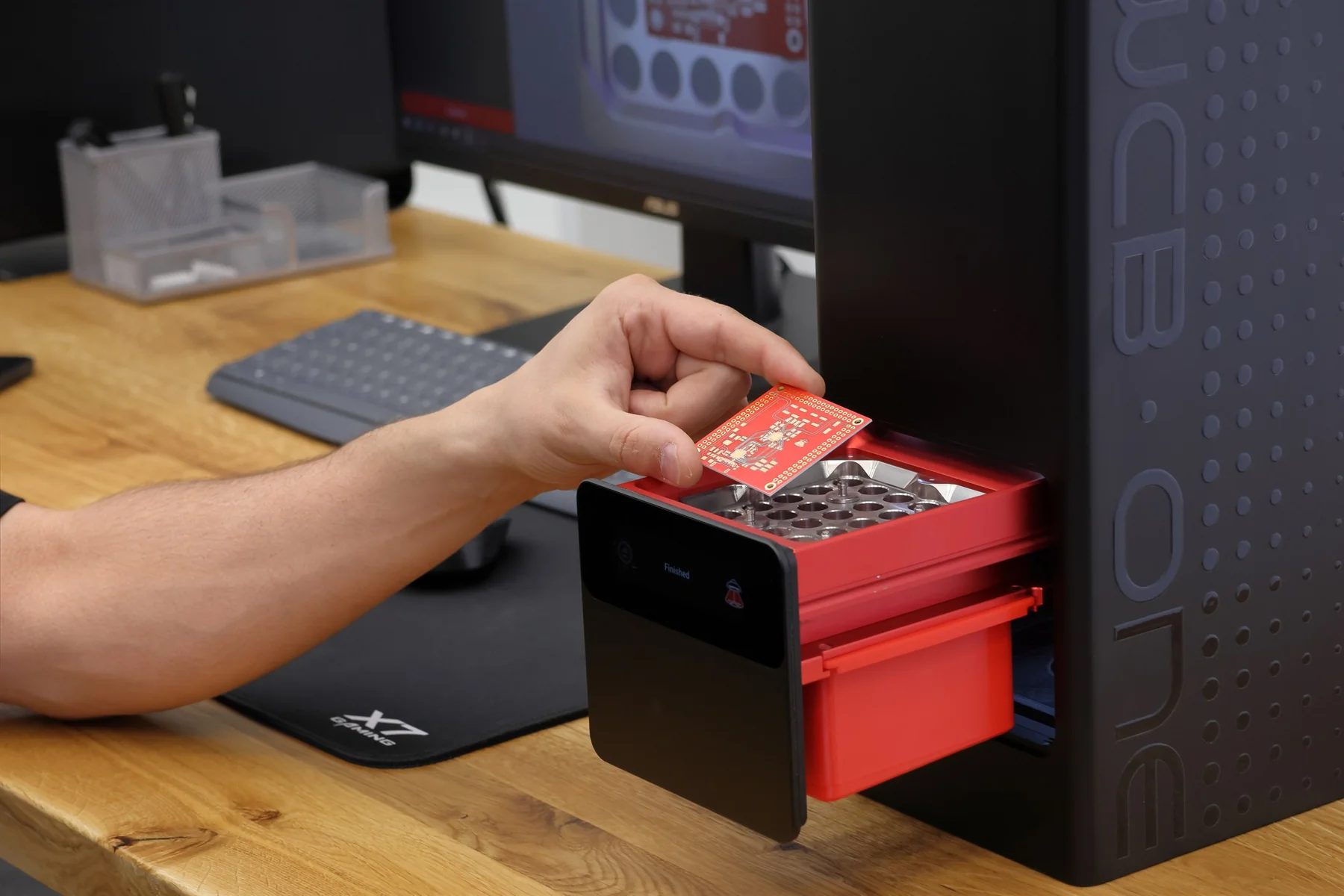
One desktop workflow, timed on our benchmark weather station board—from loading the Gerbers to flashing the firmware.
30 minutes
Open your Gerbers in the PewCB app, load a blank into the tray, and press Start.
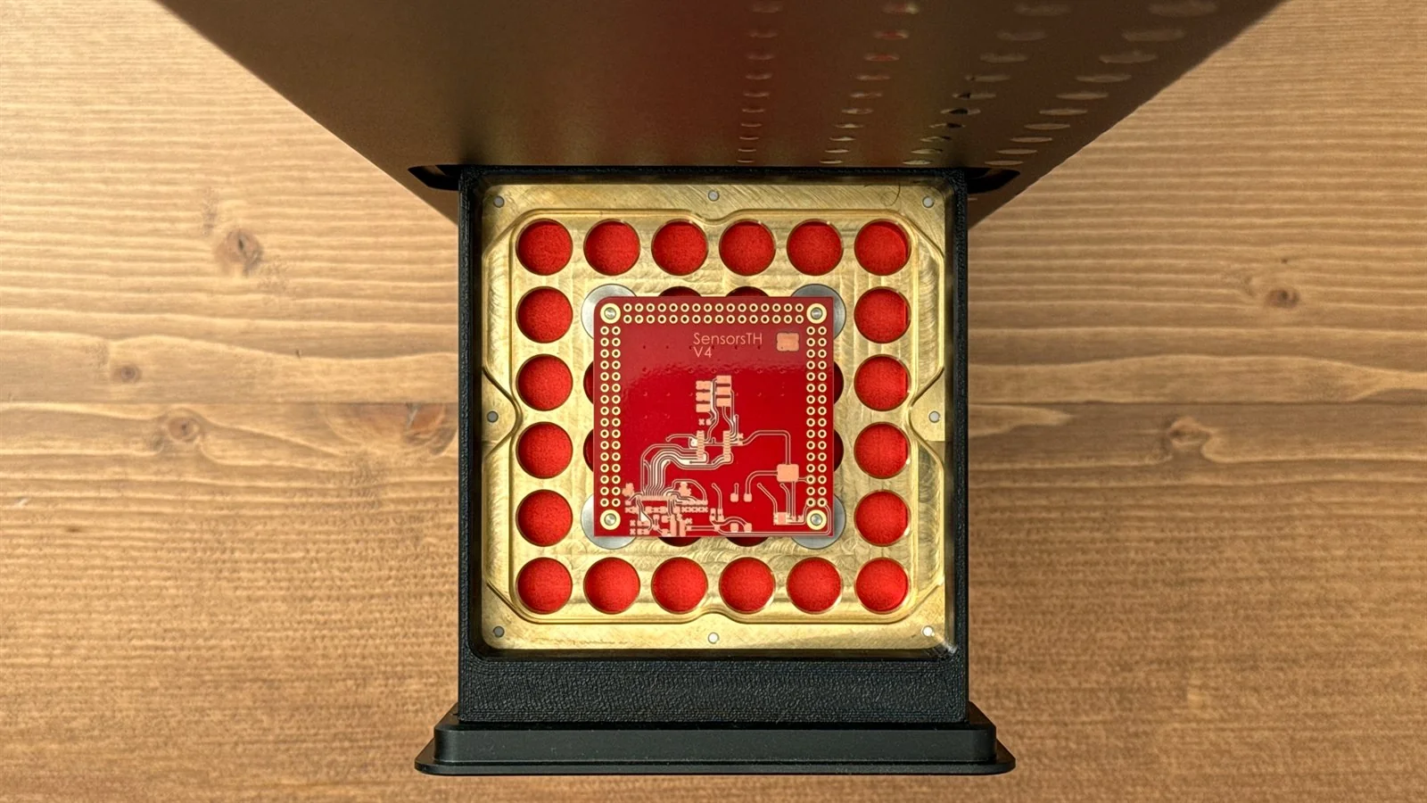
The laser forms traces, pads, and the board outline. For the second side, flip the blank onto the same mounting pins—both sides stay aligned.
10 min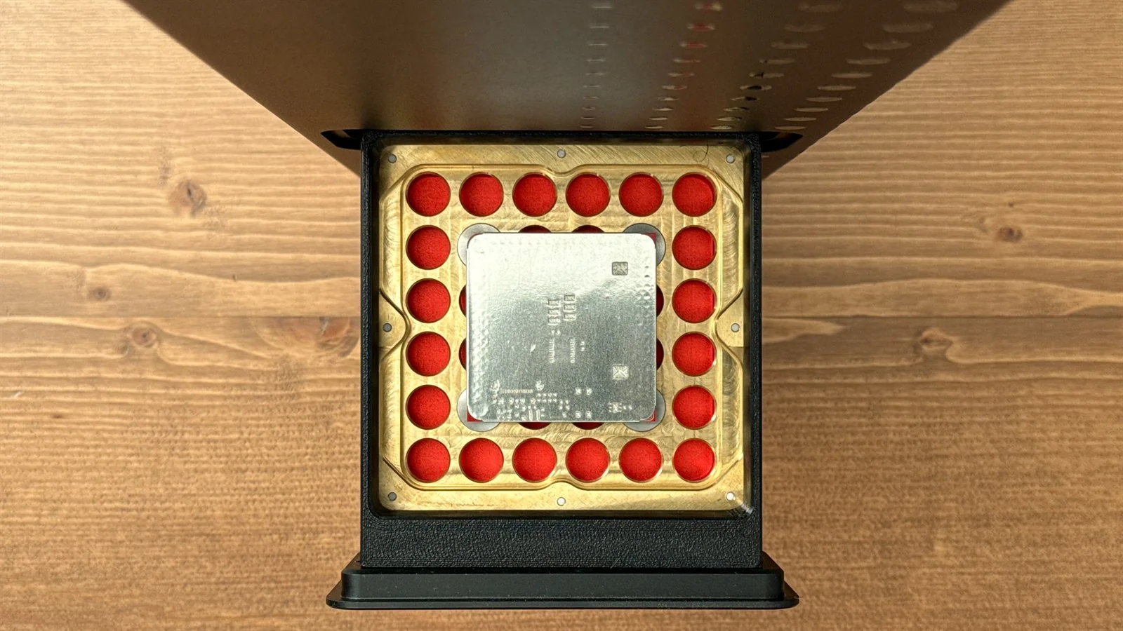
Wrap a tin stencil sheet around the board. PewCB cuts the apertures in place—spread the paste and peel the stencil off.
5 min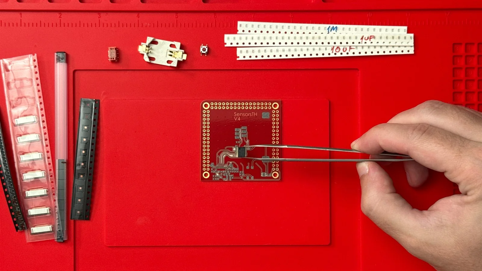
Place the components by hand with tweezers—no pick-and-place required.
10 min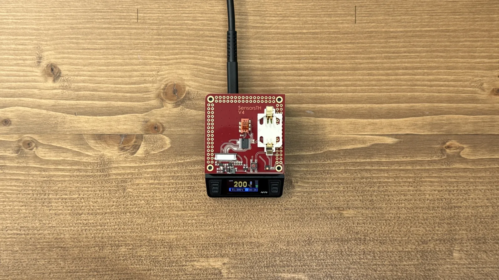
Reflow on a small hot plate—the ceramic heats quickly and evenly. Clean with IPA.
5 min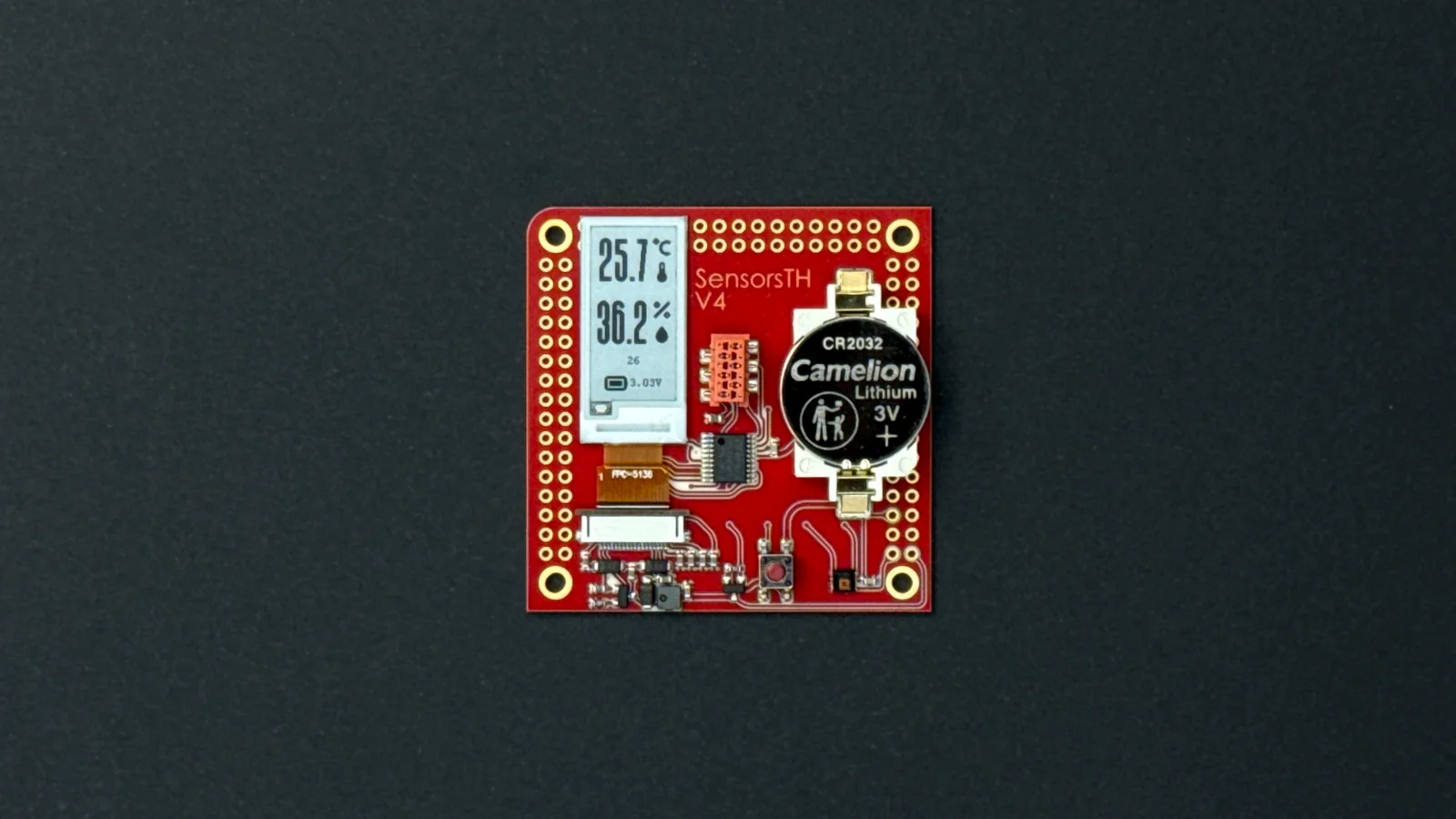
Flash the firmware, test on real hardware, and start the next iteration. Shown: our benchmark weather station—24 SMD components.
Make your next iteration today.
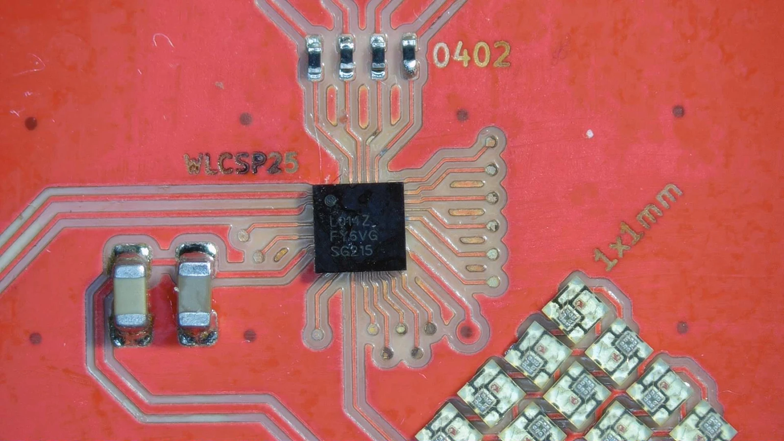
View pricing →Prototype modern SMD boards with QFN packages at 0.5 mm pitch and below, dense digital sections, and 0201 passives.
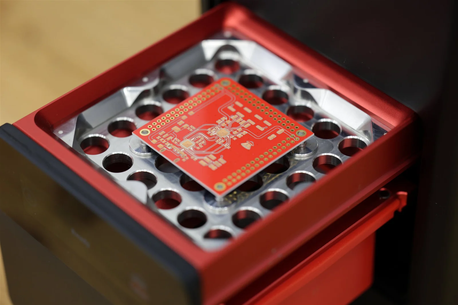
Factory calibration uses 32 sensors to correct lens distortion. Before each job, 8 platform sensors compensate for tray alignment and thermal drift.
A single-layer BGA fanout, 0201 resistors, and 1 × 1 mm addressable LEDs—made on PewCB One and assembled by hand. Solder-mask restoration lets each tiny part self-align during reflow.
Our rated 75 µm traces and clearances are guaranteed with margin. The physical limit of the process is around 25 µm.

Carefully selected blank materials deliver trace and pad quality close to factory-made PCBs—on your desk, the same day. Combined with our in-place stencil process, this gives accurate solder deposition and clean, consistent joints.

PewCB blanks combine copper foil on both sides, a ceramic substrate, pre-applied solder mask, and a grid of plated vias. The connections between layers are already built in.
Start with a matching eCAD template and route to the existing vias. The 18 µm copper foil stays firmly bonded during soldering and rework. Blanks range from 23 × 23 to 84 × 84 mm.
Need an extra layer connection? PewCB One can laser-drill additional holes for manually fitted eyelets.
Laser-cut custom outlines, holes, and cutouts—or V-score a panel and snap it apart after assembly.
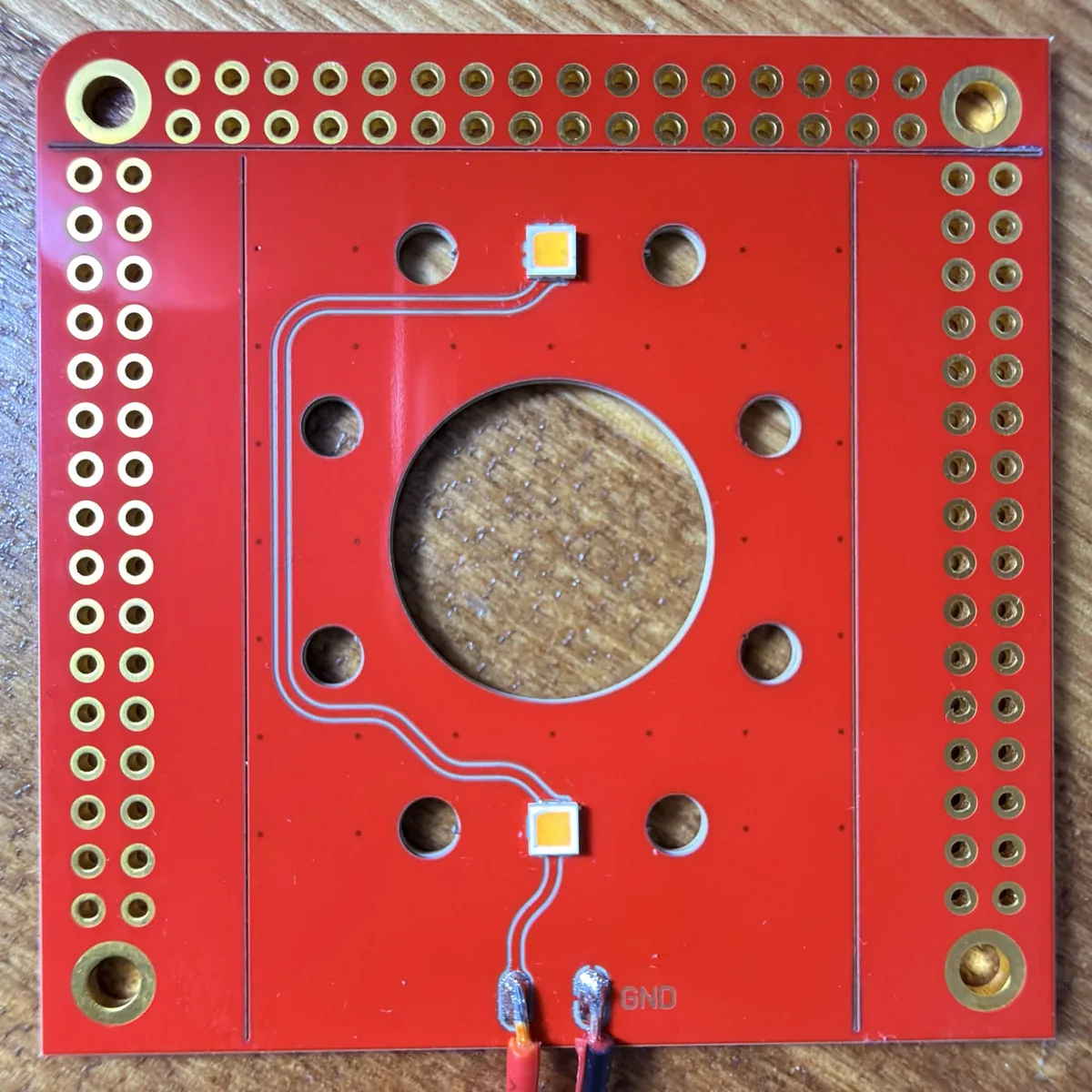
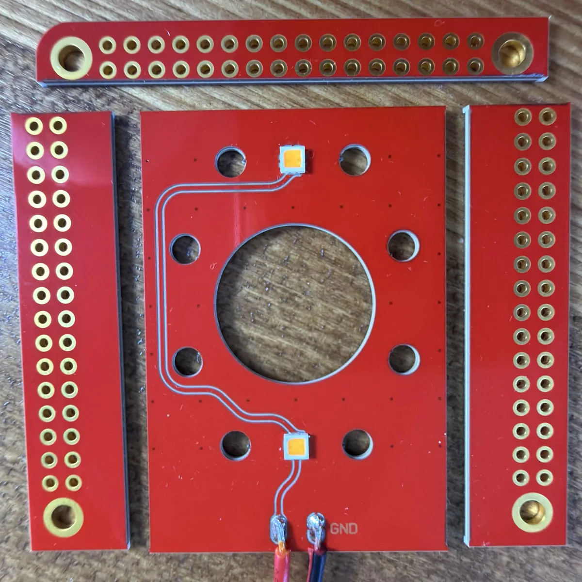
Attach a single-use stencil sheet to the finished PCB and place it back in PewCB One. The laser cuts the openings from your Gerber Paste layer directly over the pads.
The sheet stays fixed to the board during cutting and paste application. No manual alignment, frame, or jig. Apply the paste, peel off the stencil, and place the components.
Explore solder-paste stencils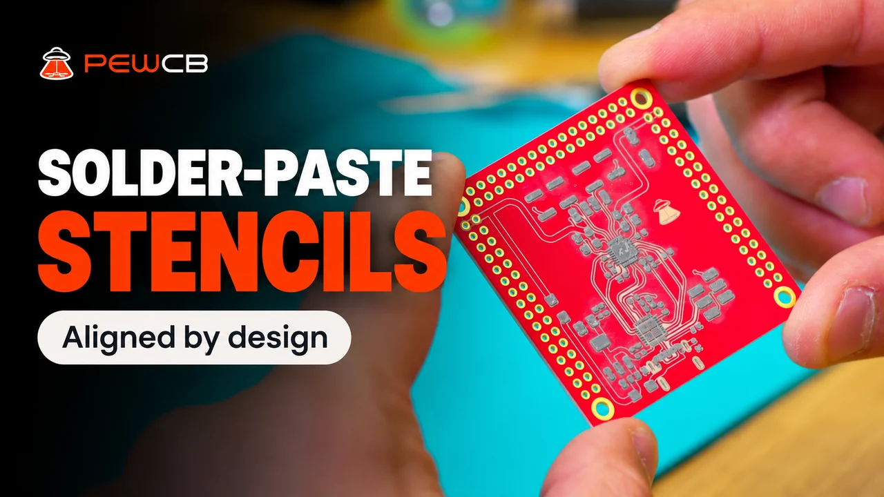
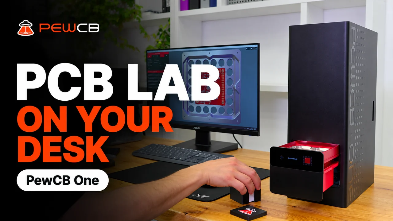
A self-contained system for your regular workspace. Just a wall outlet—no separate chemical area, external ventilation, compressed air, or vacuum line.
155 × 290 × 464 mm · 15 kg
The Class 1 enclosed laser works only with the interlocked tray closed. Follow processing through the internal camera.
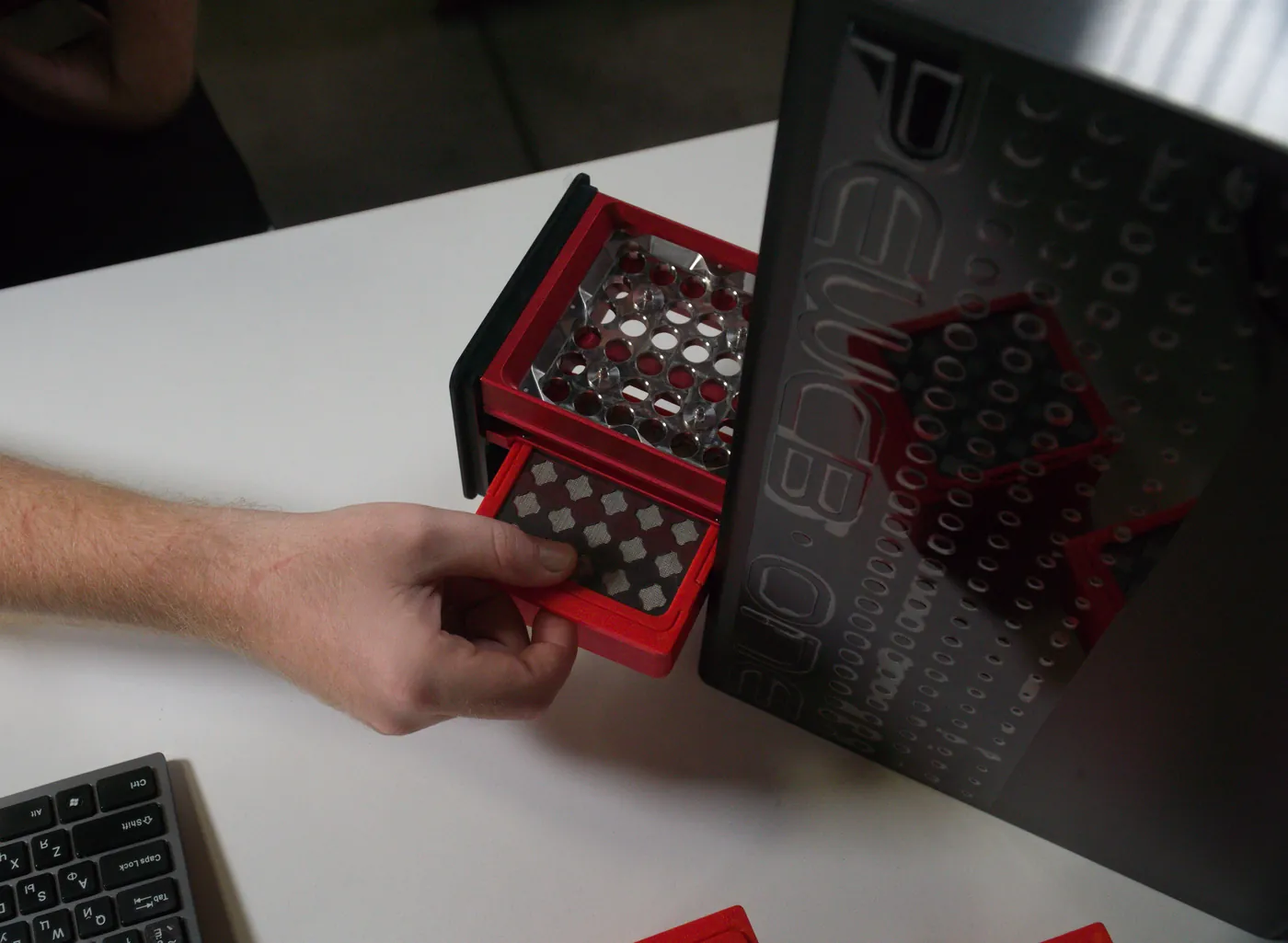
Built-in filtration
A four-stage, closed-loop filtration system is built into PewCB One. Air passes through a washable steel mesh, G4 and F7 fiber filters, and activated carbon before returning to the processing chamber.
The app tracks filter load and tells you when servicing is due. The module is accessible for cleaning and filter replacement.
The intuitive PewCB app guides you through fabrication, from opening your Gerber files to making the solder-paste stencil. Preview your board and follow clear on-screen prompts at each step.
Connect PewCB One to your Windows computer over USB. Switch to the built-in camera to check the real board inside the closed processing chamber.
Instead of spending hours checking every design decision before a week-long factory cycle, R&D teams can run bold experiments, test ideas as they emerge, and learn quickly from real hardware. With PewCB, the low cost of mistakes makes that possible.
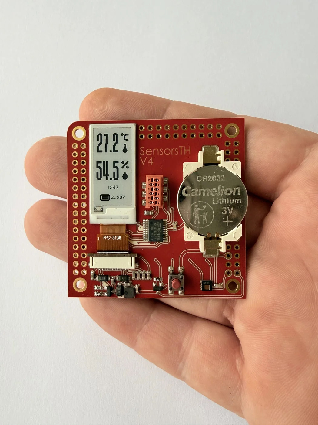
PewCB enables engineers to develop and validate key subsystems—such as voltage converters, sensors, or motor controllers—on separate, fast-to-fabricate boards. Refine each function independently, confirm performance early, and integrate proven submodules into the final product with greater confidence.
Just as 3D printers became invaluable for mechanical prototyping, PewCB unlocks a broad range of daily R&D tasks. Adapter boards, breakout boards, one-off test jigs, measurement helpers, and interface converters become practical tools when the next physical board is only about 30 minutes away.
PewCB One does not replace your PCB factory—production boards still belong there. What it removes is the cost of interruption: the days between an idea and the moment you can test it.
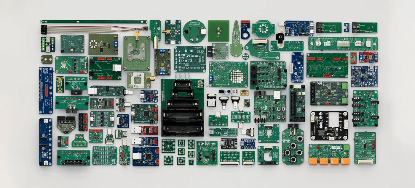
Students can design, fabricate, assemble, program, and test a PCB within a single lab session.
Shorter waits let students learn from real hardware, revise their designs, and complete the cycle while the lesson is still fresh.
Learn from real design choices. Routing errors, power integrity issues, and firmware bugs become practical lessons that students can test and fix.
EDA ➔ PCB ➔ Assembly ➔ Firmware ➔ Testing.Complete the cycle at the workstation and leave the lab with a working prototype.
An enclosed laser chamber and integrated four-stage filtration support use in classrooms, university labs, and teaching environments.
Community network
PewCB One is precise and repeatable enough that any owner can make boards for others. We are building PewFabs to bring fast prototyping to everyone—not only to those who have a machine on their desk.
Opt in as a PewFab and help engineers, students, and makers near you turn their designs into real boards.
Explore the map and find a nearby desktop fab. Contact the host about making your first board.
The faster everyone can iterate, the faster hardware moves forward. PewFabs is our way to grow that community.
Estimated delivery time: ~60 days
A 30% deposit is required to reserve the device
PewCB One machine
Blanks Starter Set — 20 pcs.
4990 USD
Shipping costs, import duties, and regional taxes are not included.
Blanks, stencil sheets, and replacement filters for your desktop workflow.
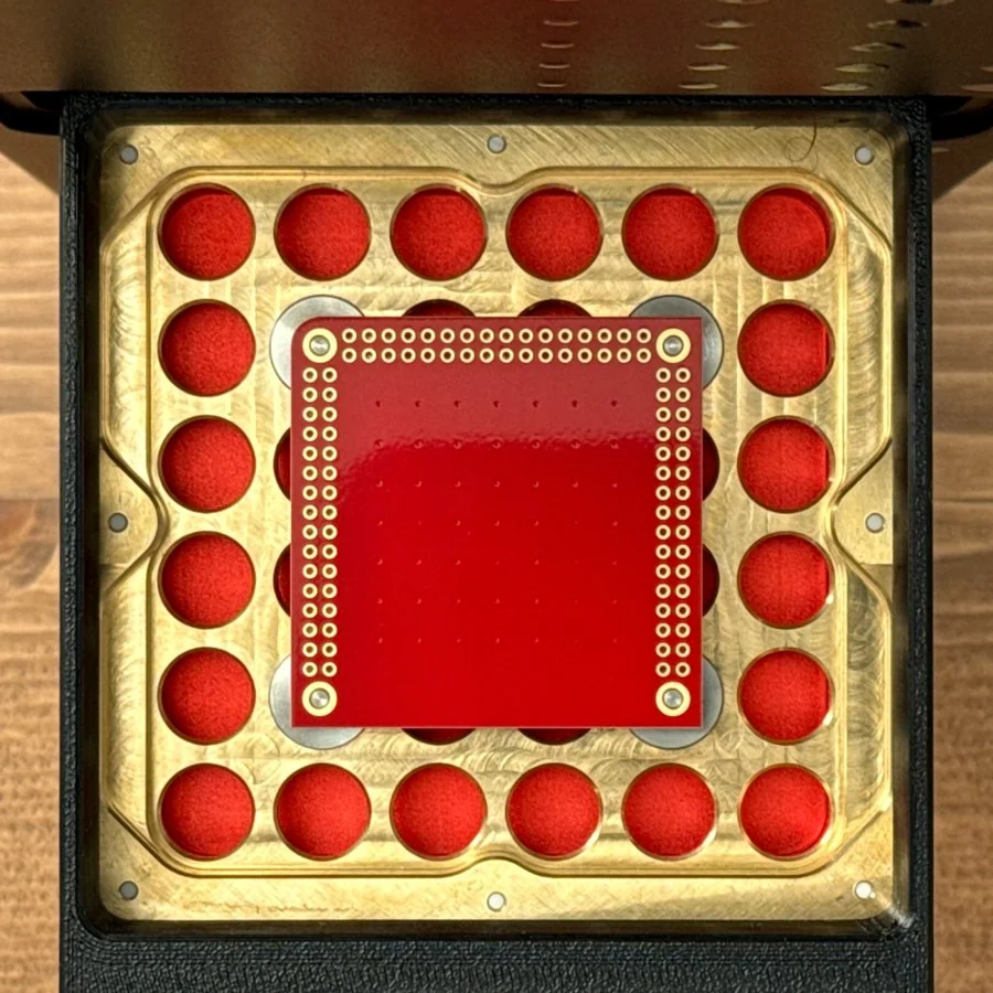
Ceramic PCB blanks with copper, solder mask, and pre-plated layer connections.
From $7 / blank
For orders of 20+ blanks.
Shipping costs, import duties, and regional taxes are not included.
Shop blanks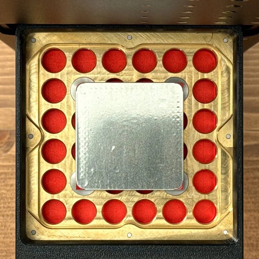
Single-use sheets for solder-paste openings cut directly over the PCB pads.
From $1 / sheet
Sheets supplied in packs of 20.
Shipping costs, import duties, and regional taxes are not included.
Shop stencil sheets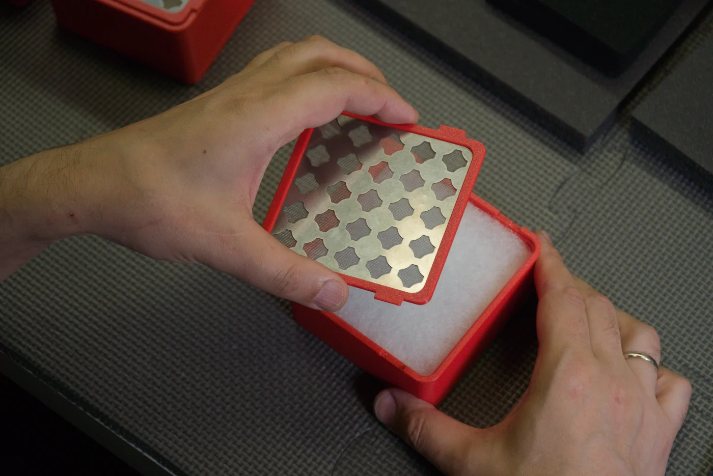
Replacement filters for the built-in air system. Keep your desktop workflow running.
Price to be announced
Availability and pricing are being finalized.
Shipping costs, import duties, and regional taxes are not included.
View filters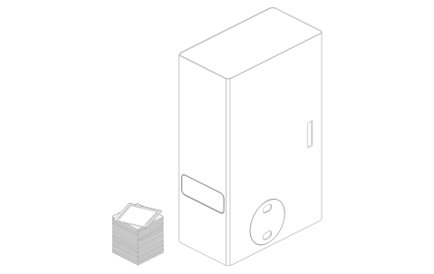
We’re engineers who build our own hardware. We know how fabrication lead times interrupt development, so we created PewCB One to speed up our own design–test–revise cycle.
The tool we needed ourselves could help other engineers, too. PewCB One became a desktop prototyping machine for engineering teams everywhere. We still use it daily—some of its own electronics were prototyped on PewCB.